| CPC H05K 1/0218 (2013.01) [H05K 1/0298 (2013.01); H05K 1/115 (2013.01); H05K 1/181 (2013.01); H05K 3/0047 (2013.01); H05K 3/303 (2013.01); H05K 3/42 (2013.01); H05K 1/0219 (2013.01); H05K 1/0231 (2013.01); H05K 1/0245 (2013.01); H05K 2201/10015 (2013.01)] | 14 Claims |
|
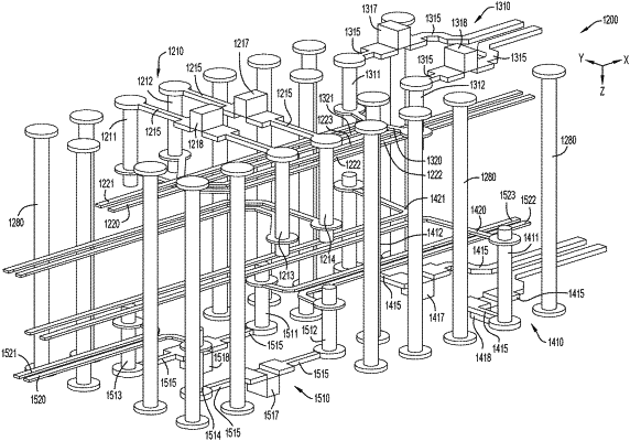
1. An apparatus comprising:
a multilayer printed circuit board comprising a stackup including an upper half of the stackup and a lower half of the stackup, the multilayer printed circuit board having a top exposed surface and a bottom exposed surface;
a first trace and via structure, having one portion disposed on the top exposed surface and another portion disposed within the upper half of the stackup;
a second trace and via structure, having one portion disposed on the top exposed surface and another portion disposed within the upper half of the stackup; and
first electrical components and second electrical components disposed on the top exposed surface of the multilayer printed circuit board and associated, respectively, with the first trace and via structure and the second trace and via structure,
wherein the first electrical components are mounted orthogonally with respect to the second electrical components,
wherein first vias of the first trace and via structure are separated by a first distance and second vias of the second trace and via structure are separated by a second distance that is less than the first distance,
wherein first traces of the first trace and via structure pass between the second vias of the second trace and via structure, and second traces of the second trace and via structure pass between the first vias of the first trace and via structure,
wherein the first electrical components overlie the second traces of the second trace and via structure, and
wherein the first traces of the first trace and via structure exposed on the top exposed surface, and to which the first electrical components are connected, are orthogonal to the second traces of the second trace and via structure.
|