| CPC H04N 25/46 (2023.01) [G06T 7/42 (2017.01); G06V 10/147 (2022.01); G06V 10/19 (2022.01); G06V 10/22 (2022.01); G06V 10/23 (2022.01); G06V 10/26 (2022.01); G06V 10/267 (2022.01); G06V 10/28 (2022.01); G06V 10/36 (2022.01); G06V 10/431 (2022.01); G06V 10/44 (2022.01); G06V 10/443 (2022.01); G06V 10/467 (2022.01); G06V 10/478 (2022.01); G06V 10/54 (2022.01); H04N 23/61 (2023.01); H04N 25/76 (2023.01); G06K 7/1413 (2013.01); G06K 7/1478 (2013.01); H04N 23/80 (2023.01); H04N 25/40 (2023.01)] | 20 Claims |
|
1. A CMOS image sensor configured to implement the capturing of an image, upon external command (trig), and to output, towards an optical code recognition system, capture image data within a corresponding image frame (DATA-OUT),
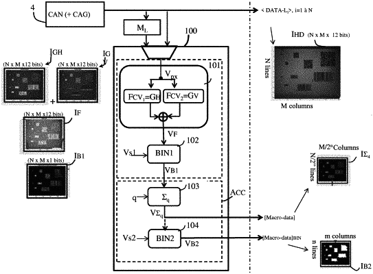
the image sensor being integrated into the same integrated circuit chip as a matrix of pixels comprising N lines and M columns and a sequential read circuit of the N lines of pixels of the matrix, wherein the sensor includes a digital processing circuit configured to apply a calculation process to the capture image data according to the acquisition of them by the sequential read circuit and in a synchronous manner, in order to calculate, on the fly, a macro-image, taking as a starting point the capture image data corresponding to the code location information in said capture image, and to transmit it to the footer of said image frame (DATA-OUT), following said capture image data,
said macro-image being such that each macro-image point corresponds to a block (B) of points of the capture image, said calculation process of the macro-image comprising at least
for each pixel of the matrix:
a first stage of calculation of at least one filter (Fcv) defined by the coefficients of a convolution mask, which establishes, for the pixel, a first numeric value (VF), corresponding to high-frequency spatial information extracted from the capture image data of said pixel and the adjacent pixels in an adjacent window delimited by the convolution mask centered on the pixel,
the calculation being carried out on the fly by the sequential read circuit of said capture image data of the respective pixel and the adjacent pixels as the acquisition progresses, said first numeric value being encoded using the same number of bits (r) as
said capture image data;
a second stage of binarisation (BIN1) of the first numeric value, establishing a first binary value (VB1) for each pixel of the matrix; and
for each block (B) of pixels of the matrix:
a third stage of calculation of a second numeric value (VΣ) by adding up said first binary values (VB1) of the pixels in the block concerned in an accumulation register of Q=b1+b2 output bits, where b1 and b2 define the number n=2b1 of lines of pixels in the block and the number m=2b2 of columns of pixels in the block, n and m being greater than 1.
|