| CPC H04M 1/0266 (2013.01) [B29C 65/48 (2013.01); B29C 66/00145 (2013.01); B29C 66/7465 (2013.01); C03B 23/023 (2013.01)] | 18 Claims |
|
1. A housing assembly comprising:
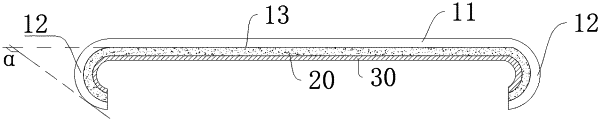
a housing body having a bottom portion and at least one side wall connected with an outer edge of the bottom portion, wherein each of the at least one side wall and the bottom portion cooperatively define a bending angle larger than 70 degrees;
a flexible film layer disposed on a first surface of the housing body, wherein the flexible film layer has an elongation at break higher than or equal to 150% and a surface energy higher than or equal to 32 dyn/cm, and the first surface of the housing body comprises a surface of the bottom portion close to the flexible film layer and a surface of the at least one side wall close to the flexible film layer; and
a decorative layer disposed on a surface of the flexible film layer away from the housing body, wherein the decorative layer comprises an ultraviolet transfer layer disposed on the surface of the flexible film layer away from the housing body and a coating layer disposed on a surface of the ultraviolet transfer layer away from the flexible film layer, wherein the coating layer comprises at least two coating sub-layers, and wherein the coating layer satisfies at least one of the following conditions:
the coating layer has a thickness smaller than or equal to 350 nm; or
a difference in thickness between each two adjacent coating sub-layers is smaller than or equal to 80 nm.
|