| CPC H03H 9/058 (2013.01) [H01L 23/66 (2013.01); H03H 3/08 (2013.01); H03H 9/25 (2013.01)] | 9 Claims |
|
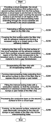
1. A method of packaging a filter chip, comprising:
providing a circuit substrate, wherein the circuit substrate comprises a first surface and a second surface remote from the first surface, wherein a circuit layer is pre-formed on the first surface, and a conductive layer covering the second surface is pre-formed on all regions of the second surface; at least one interconnecting hole extending through the circuit substrate is pre-formed in the circuit substrate;
fabricating a filtering functional layer on the filter chip;
covering the first surface and/or the filter chip with an adhesive material and forming at least one recessed cavity or at least one closed cavity in the adhesive material;
adhering the filter chip to the first surface of the circuit substrate via the adhesive material, such that at least one surface acoustic wave transmitting region of the filter chip corresponds to the at least one recessed cavity or closed cavity in the adhesive material to form a gap therebetween;
encapsulating the filter chip with an encapsulating material;
forming at least one interconnecting hole extending from the second surface to at least one pin of the filter chip to expose at least one chip pin bump or pad metal;
filling the at least one interconnecting hole with a conductive material, so that the conductive material is in electrical contact with the at least one chip pin bump or pad metal of the filter chip;
processing the conductive layer on the second surface to form a circuit layer; and
forming, on the second surface, at least one external pin pad electrically connected to the at least one chip pin bump or pad metal of the filter chip via the at least one interconnecting hole;
the covering the first surface and/or the filter chip with an adhesive material and forming at least one recessed cavity in the adhesive material comprises: covering the first surface with the adhesive material and partially removing the adhesive material to form at least one recessed cavity; and
the adhering the filter chip to the first surface of the circuit substrate via the adhesive material comprises: adhering, onto the adhesive material, the filter chip having protrusions on a side where the at least one surface acoustic wave transmitting region is located, so that the at least one surface acoustic wave transmitting region corresponds to the at least one recessed cavity in the adhesive material to form at least one gap therebetween.
|