US 11,784,394 B2
Wireless communication devices
Xiaofang Mu, Cupertino, CA (US); Annie Manuja, Sunnyvale, CA (US); Christopher D. Guichet, Mountain View, CA (US); Erik G. de Jong, San Francisco, CA (US); Jorge L. Rivera Espinoza, San Jose, CA (US); Patrick J. Crowley, San Jose, CA (US); Steven C. Roach, Martinez, CA (US); Venkatesh Rajendran, San Jose, CA (US); William C. Lukens, San Francisco, CA (US); Woojin Jung, San Mateo, CA (US); Yue Chen, San Jose, CA (US); Zhiwei Gu, Cupertino, CA (US); Derek Iwamoto, Sunnyvale, CA (US); Siddharth Nangia, San Francisco, CA (US); Scott D. Morrison, Austin, TX (US); Kevin A. Klenk, Sunnyvale, CA (US); and Neeloy Roy, San Francisco, CA (US)
Assigned to Apple Inc., Cupertino, CA (US)
Filed by Apple Inc., Cupertino, CA (US)
Filed on Dec. 7, 2021, as Appl. No. 17/544,262.
Claims priority of provisional application 63/242,868, filed on Sep. 10, 2021.
Prior Publication US 2023/0084538 A1, Mar. 16, 2023
Int. Cl. H01Q 1/24 (2006.01); H01Q 1/52 (2006.01); H01Q 9/04 (2006.01); H01Q 1/22 (2006.01)
CPC H01Q 1/24 (2013.01) [H01Q 1/22 (2013.01); H01Q 1/2283 (2013.01); H01Q 1/52 (2013.01); H01Q 1/526 (2013.01); H01Q 9/04 (2013.01); H01Q 9/0457 (2013.01)] 19 Claims
OG exemplary drawing
 
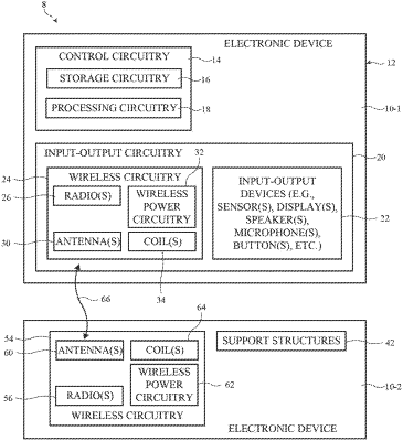
1. An electronic device having first and second opposing sides comprising:
a housing having a housing portion on the first side;
a display on the second side mounted to the housing;
a system package substrate in the housing;
a wireless communication module mounted to the system package substrate, the wireless communication module including:
a module substrate mounted to the system package substrate; and
a conductive patch on the module substrate configured to convey radio-frequency signals through the housing;
encapsulation material disposed on the system package substrate and around the wireless communication module; and
conductive shielding material disposed over the encapsulation material, the conductive shielding material defining an opening aligned with the conductive patch.