| CPC H01L 33/24 (2013.01) [H01L 33/06 (2013.01); H01L 33/30 (2013.01); H01L 33/46 (2013.01)] | 20 Claims |
|
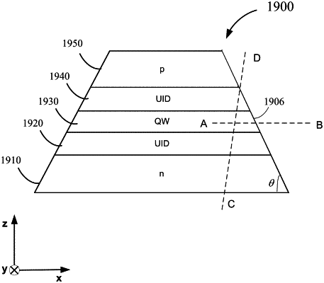
1. A micro-light emitting diode (micro-LED) device comprising a mesa structure, the mesa structure comprising:
a first set of one or more semiconductor layers;
an active layer on the first set of one or more semiconductor layers and configured to emit light;
a second set of one or more semiconductor layers on the active layer; and
a dielectric layer in sidewall regions of the mesa structure,
wherein a first thickness of a center region of the second set of one or more semiconductor layers is higher than a second thickness of a sidewall region of the second set of one or more semiconductor layers, such that a distance from a surface of the sidewall region of the second set of one or more semiconductor layers to the active layer is less than a distance from a surface of the center region of the second set of one or more semiconductor layers to the active layer to form a surface potential-induced lateral potential barrier at a sidewall region of the active layer caused by a surface potential at the sidewall region of the second set of one or more semiconductor layers;
wherein the second set of one or more semiconductor layers includes a p-type semiconductor layer and an undoped or unintentionally doped semiconductor layer between the p-type semiconductor layer and the active layer; and
wherein the p-type semiconductor layer is partially or fully removed at the sidewall region of the second set of one or more semiconductor layers to form a step structure.
|