| CPC H01L 29/7397 (2013.01) [H01L 29/0607 (2013.01)] | 20 Claims |
|
1. A semiconductor device, comprising:
a first electrode;
a second electrode, a direction from the second electrode toward the first electrode being along a first direction;
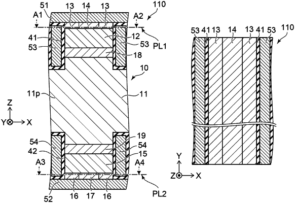
a semiconductor member located between the second electrode and the first electrode in the first direction, the semiconductor member including
a first semiconductor region of a first conductivity type,
a second semiconductor region located between the first semiconductor region and the first electrode, the second semiconductor region being of a second conductivity type,
a third semiconductor region located between the second semiconductor region and the first electrode, the third semiconductor region being of the first conductivity type,
a fourth semiconductor region located between the second semiconductor region and the first electrode, the fourth semiconductor region being of the second conductivity type and including
a first impurity concentration of the second conductivity type,
a first carrier concentration of the second conductivity type, and
a first volume ratio of a volume of the fourth semiconductor region to a volume of the semiconductor member,
a fifth semiconductor region located between the first semiconductor region and the second electrode, the fifth semiconductor region being of the second conductivity type,
a sixth semiconductor region located between the fifth semiconductor region and the second electrode, the sixth semiconductor region being of the first conductivity type; and
a seventh semiconductor region located between the fifth semiconductor region and the second electrode, the seventh semiconductor region being of the second conductivity type and including at least one of
a second impurity concentration that is of the second conductivity type and is greater than the first impurity concentration,
a second carrier concentration that is of the second conductivity type and is greater than the first carrier concentration, or
a second volume ratio that is greater than the first volume ratio and is a volume ratio of the seventh semiconductor region to the volume of the semiconductor member;
a third electrode, a second direction from a portion of the third electrode toward the second semiconductor region crossing the first direction, at least a portion of the third semiconductor region being in at least one of a first position or a second position, the first position being between the fourth semiconductor region and a portion of the third electrode in the second direction, the second position being between the portion of the third electrode and a portion of the second semiconductor region in the second direction;
a fourth electrode, a third direction from a portion of the fourth electrode toward the fifth semiconductor region crossing the first direction, at least a portion of the sixth semiconductor region being in at least one of a third position or a fourth position, the third position being between the seventh semiconductor region and a portion of the fourth electrode in the third direction, the fourth position being between the portion of the fourth electrode and a portion of the fifth semiconductor region in the third direction;
a first insulating member, at least a portion of the first insulating member being between the third electrode and the semiconductor member; and
a second insulating member, at least a portion of the second insulating member being between the fourth electrode and the semiconductor member.
|