| CPC H01L 29/66833 (2013.01) [B82Y 10/00 (2013.01); G11C 16/0466 (2013.01); G11C 16/10 (2013.01); G11C 16/14 (2013.01); H01L 29/0673 (2013.01); H01L 29/0676 (2013.01); H01L 29/40117 (2019.08); H01L 29/4234 (2013.01); H01L 29/42392 (2013.01); H01L 29/66795 (2013.01); H01L 29/792 (2013.01); H01L 29/7926 (2013.01); H01L 29/7833 (2013.01)] | 20 Claims |
|
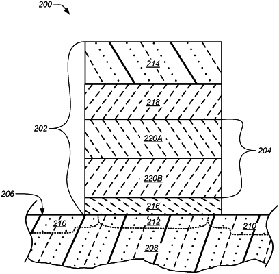
1. A method to form a non-volatile memory device, comprising:
providing a semiconductor substrate;
forming a lower dielectric layer over the semiconductor substrate;
forming a memory control gate layer on the lower dielectric layer;
forming an upper dielectric layer on the memory control gate layer, wherein the memory control gate layer is formed immediately adjacent to and sandwiched between the lower dielectric layer and the upper dielectric layer;
forming a first opening through a stack of the upper dielectric layer, the memory control gate layer and the lower dielectric layer;
forming a blocking dielectric layer, a charge storing layer and a tunnel dielectric layer in the first opening, wherein forming the charge storing layer comprising forming a first oxygen-rich silicon oxynitride layer closer to the tunnel dielectric layer and forming a second oxygen-lean silicon oxynitride layer closer to the blocking dielectric layer;
removing a blocking dielectric layer, a charge storing layer and a tunnel dielectric layer from a bottom surface of the first opening;
forming a semiconductor layer in the opening, wherein a part of the semiconductor layer forming a vertical channel region of the non-volatile memory device;
forming a dielectric filler material in the opening such that the dielectric filler material is surrounded by the semiconductor layer within the opening; and
incorporating carbon into the second oxygen-lean silicon oxynitride layer.
|