| CPC H01L 29/66462 (2013.01) [H01L 21/26553 (2013.01); H01L 29/0843 (2013.01); H01L 29/7786 (2013.01); H01L 29/2003 (2013.01)] | 11 Claims |
|
1. A method of fabricating a semiconductor device, the method comprising the steps of:
providing a semiconductor substrate that includes a plurality of epitaxial layers, including a channel layer and a permanent cap over the channel layer, wherein the permanent cap defines an upper surface of the semiconductor substrate;
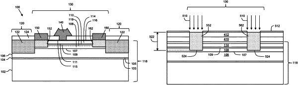
forming a sacrificial cap over the permanent cap in an active region of the device, wherein the sacrificial cap comprises a semiconductor material that includes a superlattice structure with multiple pairs of alternating layers of aluminum gallium nitride (AlGaN) and aluminum nitride (AlN), and wherein a composition of the sacrificial cap is selected to act as an etch stop during subsequent removal of a sacrificial insulating layer;
after forming the sacrificial cap, forming the sacrificial insulating layer over the sacrificial cap in the active region of the device;
forming one or more current carrying regions in the semiconductor substrate in the active region of the device by performing an ion implantation process to implant ions through the sacrificial insulating layer and the sacrificial cap, and into the semiconductor substrate;
removing the sacrificial insulating layer using a first etch process that stops at the sacrificial cap, wherein the first etch process is a dry etch process;
after removing the sacrificial insulating layer, using a second etch process to completely remove the sacrificial cap in the active region of the device, while refraining from removing the permanent cap; and
forming one or more current carrying contacts over the one or more current carrying regions.
|