| CPC H01L 29/1008 (2013.01) [H01L 29/0808 (2013.01); H01L 29/0821 (2013.01); H01L 29/401 (2013.01); H01L 29/41708 (2013.01); H01L 29/42304 (2013.01); H01L 29/6625 (2013.01); H01L 29/66242 (2013.01); H01L 29/735 (2013.01); H01L 29/737 (2013.01)] | 20 Claims |
|
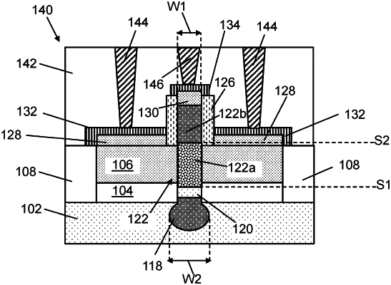
1. A lateral bipolar transistor structure comprising:
a doped semiconductor region within a substrate, the doped semiconductor region including a material composition distinct from a material composition of the substrate;
an emitter/collector (E/C) layer over an insulator over the substrate, the E/C layer having a first doping type;
a semiconductor buffer adjacent the insulator; and
a base layer on the semiconductor buffer and adjacent the E/C layer, the base layer including a lower surface below the E/C layer and an upper surface above the E/C layer, wherein the base layer has a second doping type opposite the first doping type.
|