| CPC H01L 28/90 (2013.01) [H01L 21/486 (2013.01); H01L 23/13 (2013.01); H01L 23/49816 (2013.01); H01L 23/49827 (2013.01); H01L 23/49838 (2013.01); H01L 24/16 (2013.01); H01L 24/81 (2013.01); H01L 25/16 (2013.01); H01L 2224/16225 (2013.01); H01L 2924/1433 (2013.01); H01L 2924/19041 (2013.01); H01L 2924/19102 (2013.01)] | 21 Claims |
|
1. A chip package comprising:
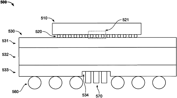
an integrated circuit die comprising a power distribution circuit configured to control distribution of power to one or more circuits of the integrated circuit die, the integrated circuit die comprising one or more capacitors extending from a surface of the integrated circuit die that includes interconnection pads, each capacitor being connected to the power distribution circuit by conductors in a manner that decouples the one or more circuits of the integrated circuit die from the power distribution circuit; and
a substrate different from the integrated circuit die and having (i) a first surface on which the integrated circuit die is mounted via the interconnection pads of the integrated circuit die and (ii) a second surface opposite the first surface, the substrate comprising one or more cavities formed in the first surface, each cavity extending from the first surface into the substrate to a third surface between the first surface and the second surface, and each cavity being configured to receive at least one of the one or more capacitors when the integrated circuit die is mounted on the first surface of the substrate,
wherein each of the one or more cavities and each of the one or more capacitors are arranged under a core power distribution area of the integrated circuit die that includes the power distribution circuit, and
wherein the core power distribution area is a partial area of the integrated circuit die that includes the power distribution circuit.
|