| CPC H01L 27/14616 (2013.01) [H01L 27/14603 (2013.01); H01L 27/14614 (2013.01); H01L 27/14641 (2013.01); H01L 27/14643 (2013.01); H01L 27/14856 (2013.01)] | 21 Claims |
|
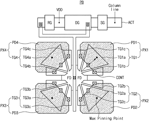
1. An image sensing device comprising:
one photoelectric conversion element configured to generate photocharges in response to incident light;
one floating diffusion region located in a vicinity of the one photoelectric conversion element and configured to temporarily store the photocharges generated by the one photoelectric conversion element; and
a transfer gate disposed to overlap with the one photoelectric conversion element and configured to transmit the photocharges generated by the one photoelectric conversion element to the one floating diffusion region,
wherein the transfer gate includes:
a first transfer gate disposed to overlap a center section of the one photoelectric conversion element, and configured to operate in response to a first potential level;
a second transfer gate located at one side of the first transfer gate; and
a third transfer gate located at another side of the first transfer gate,
wherein the second transfer gate and the third transfer gate are disposed to overlap a boundary region of the one photoelectric conversion element and configured to operate in response to a second potential level different from the first potential level,
wherein the first transfer gate, the second transfer gate, and the third transfer gate overlap different portions of the one photoelectric conversion element that is located at a certain level within a substrate, and
wherein a first portion of the one photoelectric conversion element that overlaps the first transfer gate is greater than a second portion and a third portion of the one photoelectric conversion element that overlap the second transfer gate and the third transfer gate, respectively, and
wherein each of the first transfer gate, the second transfer gate, and the third transfer gate overlaps the one floating diffusion region.
|