| US 11,784,189 B2 | ||
| Monolithic integration of diverse device types with shared electrical isolation | ||
| Francois Hebert, San Mateo, CA (US); and Handoko Linewih, (SG) | ||
| Assigned to GlobalFoundries U.S. Inc., Malta, NY (US) | ||
| Filed by GLOBALFOUNDRIES U.S. Inc., Malta, NY (US) | ||
| Filed on Aug. 20, 2021, as Appl. No. 17/407,680. | ||
| Prior Publication US 2023/0059665 A1, Feb. 23, 2023 | ||
| Int. Cl. H01L 27/12 (2006.01); H01L 21/84 (2006.01); H01L 27/085 (2006.01); H01L 29/872 (2006.01) | ||
| CPC H01L 27/1203 (2013.01) [H01L 21/84 (2013.01); H01L 27/085 (2013.01); H01L 29/872 (2013.01)] | 13 Claims |
|
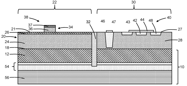
1. A structure comprising:
a substrate including a device layer, a handle substrate, and a buried insulator layer between the handle substrate and the device layer; a first semiconductor layer on the device layer in a first device region, the first semiconductor layer comprising a III-V compound semiconductor material; a second semiconductor layer on the device layer in a second device region, the second semiconductor layer comprising silicon; a high-electron-mobility transistor including a gate structure on the first semiconductor layer; and a second device structure including a doped region in the second semiconductor layer, the doped region and the second semiconductor layer defining a p-n junction. |