| CPC H01L 23/552 (2013.01) [H01L 23/49838 (2013.01); H01L 24/13 (2013.01); H01L 25/0652 (2013.01); H01L 25/18 (2013.01); H01L 25/50 (2013.01); H01L 2224/1357 (2013.01); H01L 2224/13144 (2013.01); H01L 2224/13647 (2013.01); H01L 2225/06506 (2013.01); H01L 2225/06537 (2013.01); H01L 2225/06562 (2013.01); H01L 2225/06582 (2013.01); H01L 2924/3025 (2013.01)] | 18 Claims |
|
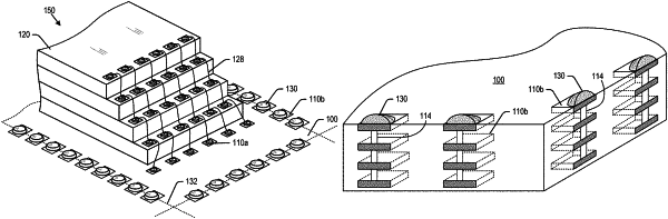
1. A semiconductor device, comprising:
a substrate comprising:
one or more conductive layers, a layer of the one or more conductive layers comprising peripheral contact pads around one or more edges of the substrate, and
conductive bumps formed on the peripheral contact pads and comprising severed edges at the one or more edges of the substrate;
one or more semiconductor dies mounted on the substrate and electrically coupled to the substrate;
an enclosure housing the one or more semiconductor dies; and
an electrically conductive coating disposed on the enclosure configured to shield the semiconductor device against the transmission and/or reception of at least one of electromagnetic interference and radio frequency interference, the electrically conductive coating electrically coupled to the severed edges of the conductive bumps;
wherein the conductive bumps are severed during singulation of the semiconductor device from a panel.
|