| CPC H01L 23/3735 (2013.01) [H01L 23/3736 (2013.01)] | 17 Claims |
|
1. A semiconductor device comprising:
a first layer having a first layer conductive contact and being doped at a first concentration of a first dopant type, the first dopant type being a P type dopant;
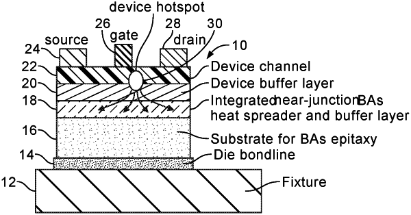
a second layer on top the first layer and being doped at a second concentration of the first dopant type, the second concentration being less than the first concentration, wherein the first layer provides improved thermal conductivity while having a coefficient of thermal expansion (CTE) matching a CTE of one or more of sapphire, GaAs, and InP;
a third layer on top of the second layer and having a third layer conductive contact and being doped with a second dopant type, the second dopant type being an N type dopant, wherein the first layer removes heat from one or more of the second layer and the third layer; and
a fourth layer on top of the third layer and having a fourth layer conductive contact and being doped with the first dopant type, wherein at least one of the first and second layers is a cubic boron arsenide (BAs) layer, wherein the third layer comprises a hot-spot, the hot-spot configured to remove heat from the third layer and from the second layer.
|