| CPC H01L 21/78 (2013.01) [H01L 21/30655 (2013.01); H01L 21/67288 (2013.01)] | 20 Claims |

|
1. A method for processing a semiconductor wafer, comprising:
providing the semiconductor wafer having semiconductor devices formed as part of the semiconductor wafer and separated from each other by spaces, wherein the semiconductor wafer has a first major surface, a second major surface opposite to the first major surface, and a material atop the second major surface;
placing the semiconductor wafer onto a first carrier substrate so that the material is interposed between the first carrier substrate and the semiconductor wafer;
plasma etching the semiconductor wafer through the spaces to form singulation lines between the semiconductor devices, wherein the material overlaps the singulation lines after the plasma etching;
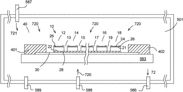
placing the semiconductor wafer within a sealed chamber, the sealed chamber adapted for reduced pressure processing;
providing a reduced pressure within the sealed chamber so that the semiconductor devices are directly exposed to the reduced pressure; and
exposing the semiconductor wafer to solvent vapors while the sealed chamber is under the reduced pressure to reduce presence of residual contaminants on the semiconductor devices and within the singulation lines resulting from the plasma etching step.
|