| CPC H01L 21/76283 (2013.01) [H10B 12/01 (2023.02); H10B 12/20 (2023.02); H10B 12/50 (2023.02)] | 9 Claims |
|
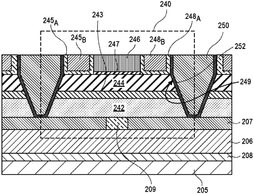
1. A transistor, comprising:
a semiconductor channel with a first surface and a second surface opposite the first surface;
a source electrode coupled to the first surface of the semiconductor channel;
a drain electrode coupled to the first surface of the semiconductor channel;
a gate dielectric over the second surface of the semiconductor channel;
a gate electrode separated from the semiconductor channel by the gate dielectric;
an isolation trench adjacent to the semiconductor channel, the isolation trench comprising a spacer lining a surface of the isolation trench, and an isolation fill material, and the isolation trench extending entirely through the gate electrode;
an etch-stop layer beneath the gate electrode and beneath the isolation trench; and
a via in the etch-stop layer, the via in contact with a bottom surface of the gate electrode.
|