| CPC G09G 3/3233 (2013.01) [G09G 3/3266 (2013.01); G11C 19/287 (2013.01); G09G 2300/0408 (2013.01); G09G 2300/0819 (2013.01); G09G 2300/0852 (2013.01); G09G 2310/0286 (2013.01)] | 22 Claims |
|
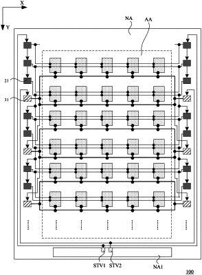
1. An array substrate with a display area and a non-display area surrounding the display area, comprising:
a plurality of pixel circuits arranged in an array along a first direction and a second direction, wherein the plurality of pixel circuits are disposed in the display area and the first direction intersects the second direction;
a first gate driving circuit in the non-display area, wherein the first gate driving circuit includes a plurality of first shift register units in cascade connection; and
a second gate driving circuit in the non-display area, the second gate driving circuit and the first gate driving circuit being at a same side of the display area, wherein the second gate driving circuit includes a plurality of second shift register units in cascade connection,
wherein:
the first gate driving circuit and the second gate driving circuit are electrically connected to different transistors in the plurality of pixel circuits; and
an orthographic projection of the first gate driving circuit on a plane of the array substrate at least partially overlaps with an orthographic projection of the second gate driving circuit on the plane of the array substrate along the second direction, and at least two of the plurality of first shift register units of the first gate driving circuit are adjacent to each other.
|