| CPC G06F 30/323 (2020.01) [G06F 30/327 (2020.01); G06F 30/392 (2020.01); G06F 2115/06 (2020.01)] | 20 Claims |
|
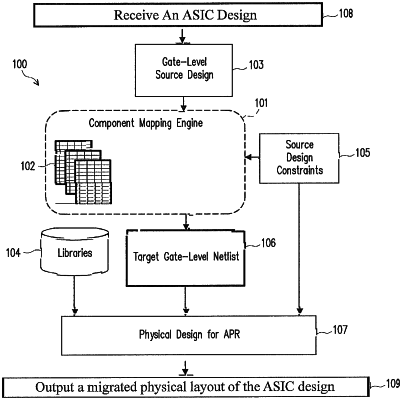
1. A method for migrating a circuit design from a first semiconductor fabrication process to a second semiconductor fabrication process comprising:
receiving the circuit design, wherein the circuit design comprises a gate-level netlist;
parsing the gate-level netlist one row at a time into one or more standard cells forming an application specific integrated circuit (ASIC) design;
forming a plurality of mapping tables having mapping rules for mapping the parsed one or more standard cells to equivalent target standard cells implemented in the second semiconductor fabrication process;
mapping the parsed one or more standard cells to the equivalent target standard cells using the plurality of mapping tables;
generating a target gate-level netlist describing the circuit design in terms of the equivalent target standard cells; and
outputting migrated physical layout of the circuit design for manufacturing under the second semiconductor fabrication process.
|