| CPC G06F 11/1441 (2013.01) [G06F 1/28 (2013.01); G06F 11/3034 (2013.01); G06F 11/3062 (2013.01); G06F 11/3495 (2013.01); G06F 2201/805 (2013.01)] | 17 Claims |
|
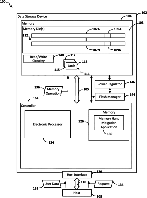
1. A data storage device, comprising:
a solid-state memory block including
a plurality of arrays, each array of the plurality of arrays including a plurality of memory devices, wherein each of the plurality of memory devices includes a plurality of memory dies, and
a plurality of power regulators,
wherein each array of the plurality of arrays is coupled to a respective one of the plurality of power regulators; and
a controller configured to:
determine whether a first array of the plurality of arrays is in a non-responsive condition,
instruct a first power regulator of the plurality of power regulators providing power to the first array to cycle power to the first array in response to determining that the first array is in the non-responsive condition,
determine whether the first array is in a responsive condition after cycling power to the first array;
stop monitoring a voltage of a power input to the memory block in response to determining that the first array is in a non-responsive condition; and
resume monitoring the voltage of the power input to the memory block after cycling power to the first array.
|