| CPC G03F 7/094 (2013.01) [G03F 7/0045 (2013.01); G03F 7/091 (2013.01); G03F 7/11 (2013.01); H01L 21/0276 (2013.01); H01L 21/3065 (2013.01); H01L 21/3085 (2013.01); H01L 21/3086 (2013.01); H01L 21/3088 (2013.01)] | 10 Claims |

|
1. A method of patterning a substrate, the method comprising:
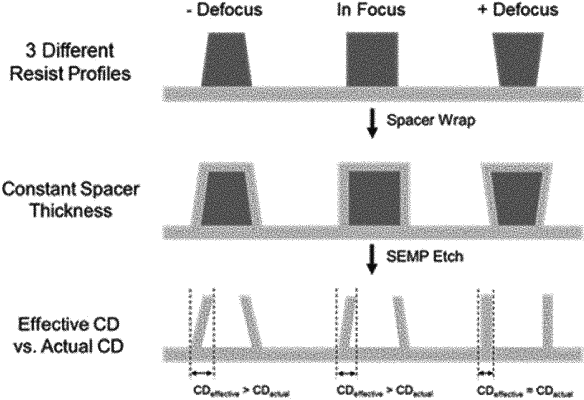
forming a patterned photoresist structure on the substrate, the patterned photoresist structure having a sidewall with a predetermined sidewall slope that corresponds to a target critical dimension (CD) for a substrate feature to be formed in the substrate;
depositing a conformal layer of spacer material on the sidewall such that the spacer material on the sidewall has a first effective CD which is different from the target CD;
removing the patterned photoresist structure from the substrate such that the spacer material remains as a sidewall spacer formed on the substrate, wherein the removing relaxes mechanical stress in the spacer material such that the sidewall spacer has a second effective CD; and
directionally etching the substrate using the sidewall spacer as an etch mask to form the substrate feature having the second effective CD in the substrate, wherein the second effective CD is closer to the target CD than the first effective CD.
|