| CPC G02F 1/136213 (2013.01) [G02F 1/13439 (2013.01); G02F 1/136227 (2013.01); G02F 1/136286 (2013.01); H01L 27/124 (2013.01); H01L 27/1248 (2013.01); H01L 27/1255 (2013.01)] | 20 Claims |
|
1. An array substrate, comprising:
a base substrate; and
a gate metal layer and a source-drain metal layer stacked in sequence on the base substrate;
wherein:
the gate metal layer comprises:
a plurality of gate lines that are independent of each other; and
a plurality of dummy gates that are independent of each other;
the source-drain metal layer comprises:
a plurality of data lines that are independent of each other; and
a plurality of dummy drains that are independent of each other;
wherein:
the dummy gate comprises:
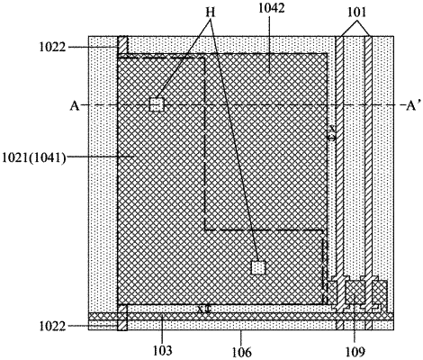
a main body portion in a pixel region defined by a gate line and a data line, wherein an orthographic projection of the main body portion on the base substrate is in an “L” shape; and
a lead-out portion; and
the dummy drains are in pixel regions, and the dummy drain in the pixel region comprises:
a first subsection overlapping with the main body portion; and
a second subsection not overlapping with the main body portion, wherein an opposite capacitance is between the first subsection and the main body portion and a coupling capacitance is between the second subsection and the main body portion; the second subsection surrounds the first subsection by half; and an orthographic projection of the first subsection on the base substrate is in an “L” shape, and an orthographic projection of the second subsection on the base substrate and the orthographic projection of the first subsection on the base substrate complement each other to form a rectangle.
|