US 11,782,199 B2
Metal-dielectric optical filter, sensor device, and fabrication method
Georg J. Ockenfuss, Santa Rosa, CA (US); Tim Gustafson, Santa Rosa, CA (US); Jeffrey James Kuna, San Francisco, CA (US); Markus Bilger, Santa Rosa, CA (US); and Richard A. Bradley, Jr., Santa Rosa, CA (US)
Assigned to VIAVI Solutions Inc., Chandler, AZ (US)
Filed by VIAVI Solutions Inc., San Jose, CA (US)
Filed on Jan. 19, 2021, as Appl. No. 17/248,285.
Application 17/248,285 is a continuation of application No. 16/266,913, filed on Feb. 4, 2019, granted, now 10,928,570.
Application 16/266,913 is a continuation of application No. 14/308,343, filed on Jun. 18, 2014, granted, now 10,197,716, issued on Feb. 5, 2019.
Application 14/308,343 is a continuation in part of application No. 13/720,728, filed on Dec. 19, 2012, granted, now 9,448,346, issued on Sep. 20, 2016.
Prior Publication US 2021/0141133 A1, May 13, 2021
Int. Cl. G02B 5/28 (2006.01); H01L 27/146 (2006.01); G02B 1/10 (2015.01)
CPC G02B 5/285 (2013.01) [G02B 1/10 (2013.01); G02B 5/281 (2013.01); G02B 5/283 (2013.01); H01L 27/14621 (2013.01); H01L 27/14685 (2013.01)] 20 Claims
OG exemplary drawing
 
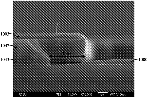
1. A method comprising:
applying a photoresist layer onto a substrate;
forming, in the photoresist layer surrounding a region of the substrate, an overhang by patterning the photoresist layer in a manner that uncovers the region; and
lifting the photoresist layer in a manner that provides a clean lift-off of the photoresist layer without breaking a coating that covers the overhang.