| CPC G01R 33/072 (2013.01) [G01R 33/0052 (2013.01); G01R 33/077 (2013.01); H10N 52/01 (2023.02); H10N 52/101 (2023.02); H10N 52/80 (2023.02)] | 21 Claims |
|
1. A microelectronic device, comprising:
a substrate including a semiconductor material; and
a Hall sensor, including:
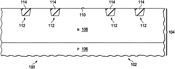
a Hall plate in the semiconductor material, the Hall plate having a first conductivity type;
a contact region of the Hall sensor in the semiconductor material contacting the Hall plate, the contact region having the first conductivity type;
an isolation structure including dielectric material on two opposite sides of the contact region, the isolation structure being laterally separated from the contact region by a gap, the isolation structure contacting the semiconductor material; and
a conductive spacer of electrically conductive material over the gap, the conductive spacer being separated from the semiconductor material by an insulating layer.
|