Ic with graphene fet sensor array patterned in layers above circuitry formed in a silicon based cmos wafer
Brett R. Goldsmith, San Diego, CA (US); Mitchell Lerner, San Diego, CA (US); and Paul Hoffman, San Diego, CA (US)
Assigned to Cardea Bio, Inc., San Diego, CA (US)
Filed by Cardea Bio, Inc., San Diego, CA (US)
Filed on Nov. 17, 2021, as Appl. No. 17/528,540.
Application 17/528,540 is a continuation of application No. 17/329,090, filed on May 24, 2021, granted, now 11,536,722.
Application 17/329,090 is a continuation of application No. 16/586,964, filed on Sep. 28, 2019, granted, now 11,016,088, issued on May 25, 2021.
Application 16/586,964 is a continuation of application No. 16/014,838, filed on Jun. 21, 2018, granted, now 10,429,381, issued on Oct. 1, 2019.
Application 16/014,838 is a continuation of application No. 15/256,493, filed on Sep. 2, 2016, granted, now 10,006,910, issued on Jun. 26, 2018.
Application 15/256,493 is a continuation in part of application No. 15/239,800, filed on Aug. 17, 2016, granted, now 9,857,328, issued on Jan. 2, 2018.
Application 15/239,800 is a continuation in part of application No. 15/225,764, filed on Aug. 1, 2016, granted, now 10,020,300, issued on Jul. 10, 2018.
Application 15/239,800 is a continuation in part of application No. 15/225,764, filed on Aug. 1, 2016, granted, now 10,020,300, issued on Jul. 10, 2018.
Application 15/225,764 is a continuation in part of application No. 15/182,533, filed on Jun. 14, 2016, granted, now 9,859,394, issued on Jan. 2, 2018.
Application 15/239,800 is a continuation in part of application No. 15/182,533, filed on Jun. 14, 2016, granted, now 9,859,394, issued on Jan. 2, 2018.
Application 15/256,493 is a continuation in part of application No. 15/182,533, filed on Jun. 14, 2016, granted, now 9,859,394, issued on Jan. 2, 2018.
Application 15/225,764 is a continuation in part of application No. 15/065,744, filed on Mar. 9, 2016, granted, now 9,618,474, issued on Apr. 11, 2017.
Application 15/256,493 is a continuation in part of application No. 15/065,744, filed on Mar. 9, 2016, granted, now 9,618,474, issued on Apr. 11, 2017.
Application 15/182,533 is a continuation in part of application No. 15/065,744, filed on Mar. 9, 2016, granted, now 9,618,474, issued on Apr. 11, 2017.
Application 15/239,800 is a continuation in part of application No. 15/065,744, filed on Mar. 9, 2016, granted, now 9,618,474, issued on Apr. 11, 2017.
Application 15/065,744 is a continuation in part of application No. 14/963,253, filed on Dec. 9, 2015, granted, now 10,429,342, issued on Oct. 1, 2019.
Application 15/225,764 is a continuation in part of application No. 14/963,253, filed on Dec. 9, 2015, granted, now 10,429,342, issued on Oct. 1, 2019.
Application 15/256,493 is a continuation in part of application No. 14/963,253, filed on Dec. 9, 2015, granted, now 10,429,342, issued on Oct. 1, 2019.
Application 15/065,744 is a continuation in part of application No. 14/963,253, filed on Dec. 9, 2015, granted, now 10,429,342, issued on Oct. 1, 2019.
Claims priority of provisional application 62/215,018, filed on Sep. 6, 2015.
Claims priority of provisional application 62/214,912, filed on Sep. 5, 2015.
Claims priority of provisional application 62/214,892, filed on Sep. 4, 2015.
Claims priority of provisional application 62/214,850, filed on Sep. 4, 2015.
Claims priority of provisional application 62/214,910, filed on Sep. 4, 2015.
Claims priority of provisional application 62/214,901, filed on Sep. 4, 2015.
Claims priority of provisional application 62/213,117, filed on Sep. 2, 2015.
Claims priority of provisional application 62/213,112, filed on Sep. 2, 2015.
Claims priority of provisional application 62/213,151, filed on Sep. 2, 2015.
Claims priority of provisional application 62/206,372, filed on Aug. 18, 2015.
Claims priority of provisional application 62/206,814, filed on Aug. 18, 2015.
Claims priority of provisional application 62/205,803, filed on Aug. 17, 2015.
Claims priority of provisional application 62/206,228, filed on Aug. 17, 2015.
Claims priority of provisional application 62/206,224, filed on Aug. 17, 2015.
Claims priority of provisional application 62/206,166, filed on Aug. 17, 2015.
Claims priority of provisional application 62/205,808, filed on Aug. 17, 2015.
Claims priority of provisional application 62/199,987, filed on Aug. 1, 2015.
Claims priority of provisional application 62/175,649, filed on Jun. 15, 2015.
Claims priority of provisional application 62/175,384, filed on Jun. 14, 2015.
Claims priority of provisional application 62/175,351, filed on Jun. 14, 2015.
Claims priority of provisional application 62/130,621, filed on Mar. 10, 2015.
Claims priority of provisional application 62/130,601, filed on Mar. 9, 2015.
Claims priority of provisional application 62/130,598, filed on Mar. 9, 2015.
Claims priority of provisional application 62/130,594, filed on Mar. 9, 2015.
Claims priority of provisional application 62/094,016, filed on Dec. 18, 2014.
Prior Publication US 2022/0155289 A1, May 19, 2022
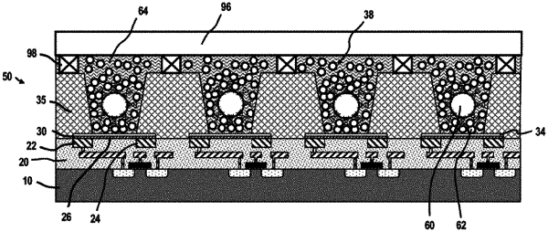
read out integrated circuit (“ROIC”) circuitry formed in a silicon based CMOS wafer that includes a top layer of dielectric material that acts as a first insulating layer between the CMOS wafer and at least one graphene field effect transistor (“gFET”) sensor array added above the CMOS wafer;
access transistors controlled by circuits of the ROIC circuitry for accessing corresponding sensing transistors of the at least one gFET sensor array, the access transistors formed in the CMOS wafer and individually comprising:
a conductive gate associated with a gate dielectric that acts as an insulating barrier separating the gate from a semiconductor channel, the semiconductor channel being formed by charge carriers in a silicon based semiconductor material connecting a source region and a drain region when a threshold gate voltage is applied;
a conductive source contact coupled to a source region at a first end of the semiconductor channel;
a conductive drain contact coupled to a drain region at a second end of the semiconductor channel; and
sensing circuitry added to the CMOS wafer and comprising graphene field effect transistors (“gFETs”) of at least one gFET sensor array, the gFETs serving as the sensing transistors and individually comprising:
a graphene channel patterned in a two-dimensional (2D) layer of graphene transferred from a growth substrate to a first insulating layer at a top surface of the CMOS wafer;
a gFET drain patterned in a conductive layer; and
a gFET source patterned in the conductive layer,
wherein the graphene channel extends between the gFET source and the gFET drain; and
a second insulating layer that acts as a passivation layer added above the gFET sources and the gFET drains of the sensor array, the second insulating layer patterned to form a passivation opening that allows direct contact of a sample liquid with the graphene channels of the gFETs, such that a liquid gate is formed above the graphene channel upon receipt of the sample liquid.