| CPC G01N 27/4145 (2013.01) | 21 Claims |
|
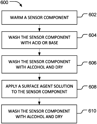
1. A method of preparing a sensor component, the method comprising:
flowing a wash solution over a sensor device, the sensor device including:
a sensor array; each sensor in the sensor array having a sensor surface comprising a metal, metal or semi-metal oxide, or metal or semi-metal nitride; and
an array of wells formed over and operatively coupled to the sensor array, each well providing a sidewall of a reaction site; and
applying a surface agent to the sensor device, the surface agent including:
a first moiety reactive with the sensor surface, the sidewall, or combinations thereof;
the first moiety including phosphate, phosphonic acid, phosphinic acid, and phosphonate, or any combination thereof; and
a second moiety distal from the first moiety comprising a positively charged functional group.
|