| CPC B41J 2/04536 (2013.01) [B41J 2/0458 (2013.01); B41J 2/04541 (2013.01); B41J 2/04555 (2013.01); B41J 2/04563 (2013.01); B41J 2/04586 (2013.01); G06F 3/1293 (2013.01); G06F 13/1668 (2013.01); G11C 7/1069 (2013.01); G11C 16/10 (2013.01); G11C 16/26 (2013.01); G11C 2207/105 (2013.01)] | 50 Claims |
|
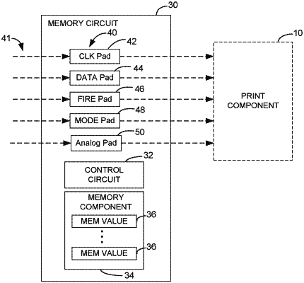
1. A replacement memory circuit for a print component comprising a fluidic die, the memory circuit being separate from the fluidic die to replace memory on the fluidic die, the memory circuit comprising:
a plurality of I/O pads, including an analog pad, to connect to a plurality of signal paths that are to communicate operating signals to and/or from the print component;
a controllable selector connected in line with said one of the signal paths via the I/O pads, the selector controllable to interrupt the corresponding signal path to the print component;
a memory component to store memory values to be associated with the print component; and
a control circuit, in response to a sequence of operating signals received by the I/O pads representing a memory read, to:
operate the controllable selector to interrupt the signal path to the fluidic die; and
provide an analog signal to the analog pad having an analog electrical value representing at least one memory value stored on the memory component corresponding to the sequence of operating signals representing a memory read.
|