| CPC B24B 37/005 (2013.01) [B24B 37/27 (2013.01); B24B 49/105 (2013.01); G01B 7/10 (2013.01)] | 19 Claims |
|
1. A method of chemical mechanical polishing, comprising:
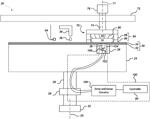
bringing a substrate having a conductive layer disposed over a semiconductor wafer into contact with a polishing pad;
receiving a base signal value representing a conductivity of the semiconductor wafer;
generating relative motion between the substrate and the polishing pad;
monitoring the substrate with an in-situ electromagnetic induction monitoring system as the conductive layer is polished to generate a sequence of signal values that depend on a thickness of the conductive layer and the conductivity of the semiconductive wafer; and
determining a sequence of thickness values for the conductive layer based on the sequence of signal values, wherein determining the sequence of thickness values including at least partially compensating for a contribution of conductivity of the semiconductor wafer to the signal values using the base signal value.
|