| CPC H01L 21/76877 (2013.01) [H01L 21/31144 (2013.01); H01L 21/76802 (2013.01); H01L 21/7684 (2013.01); H01L 21/76843 (2013.01); H01L 23/53238 (2013.01)] | 18 Claims |

|
1. A method, comprising:
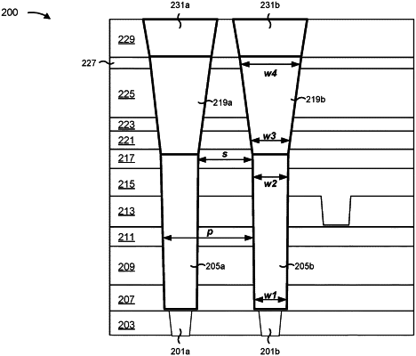
performing a first etching of a dielectric layer to produce a first recess and a second recess, wherein at least one the first recess or the second recess comprises an upper portion and a lower portion having a width less than a width of the upper portion, wherein the upper portion of the first recess is physically separated from the upper portion of the second recess by a hardmask layer;
forming, on the hardmask layer, a recovery layer comprising at least one of a polymer of a chemical form CxHy, a material including tin (Sn), or a combination of titanium fluoride (TiF) and a cyano group (CN−);
performing a second etching of the dielectric layer to expose a first back end of line (BEOL) conductive structure within the first recess and a second BEOL conductive structure within the second recess, wherein the recovery layer reduces etching of the hardmask layer during the second etching of the dielectric layer; and
forming a first conductive structure within the first recess and a second conductive structure within the second recess.
|