| CPC H05K 3/4679 (2013.01) [H05K 1/144 (2013.01); H05K 2201/10128 (2013.01); H05K 2203/104 (2013.01)] | 18 Claims |
|
1. A method of manufacturing a display device, the method comprising:
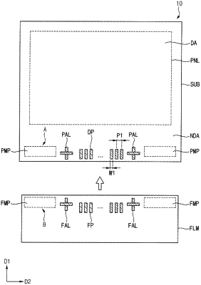
preparing a substrate including a display area and a non-display area disposed adjacent to the display area;
forming first panel magnetic patterns overlapping the non-display area and extending in a first direction on the substrate;
forming first film magnetic patterns extending in the first direction on a film;
inputting a first magnetism to the first panel magnetic patterns so that the first panel magnetic patterns have a first magnetic property;
inputting a second magnetism to the first film magnetic patterns so that the first film magnetic patterns have a second magnetic property;
aligning the film on the substrate so that the first film magnetic patterns overlap the first panel magnetic patterns in a plan view;
forming second panel magnetic patterns extending in the first direction and disposed between the first panel magnetic patterns; and
forming second film magnetic patterns extending in the first direction and disposed between the first film magnetic patterns.
|