| CPC H01L 29/36 (2013.01) [H01L 21/02236 (2013.01); H01L 21/02381 (2013.01); H01L 21/2236 (2013.01); H01L 21/2253 (2013.01); H01L 21/26513 (2013.01); H01L 29/167 (2013.01)] | 16 Claims |
|
1. A semiconductor device, comprising:
a semiconductor substrate comprising a first dopant and a second dopant, wherein a covalent atomic radius of a material of the semiconductor substrate is i) larger than a covalent atomic radius of the first dopant and smaller than a covalent atomic radius of the second dopant, or ii) smaller than the covalent atomic radius of the first dopant and larger than the covalent atomic radius of the second dopant;
a semiconductor layer on the semiconductor substrate; and
semiconductor device elements in the semiconductor layer,
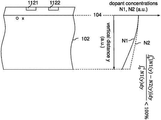
wherein a vertical concentration profile of the first dopant decreases along at least 80% of a distance between an interface of the semiconductor substrate and the semiconductor layer to a surface of the semiconductor substrate opposite to the interface,
wherein the vertical concentration profile N1(y) of the first dopant and a vertical concentration profile N2(y) of the second dopant satisfy:
 where t is a final thickness of the semiconductor substrate.
|