| CPC H10K 59/60 (2023.02) [H10K 50/865 (2023.02); H10K 59/351 (2023.02); H10K 59/50 (2023.02)] | 18 Claims |
|
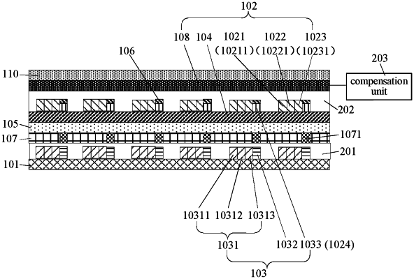
1. An array substrate, comprising a substrate, a pixel unit and a measurement unit on the substrate, and a compensation element,
wherein the measurement unit comprises:
a photosensitive device configured to detect a luminous intensity of the pixel unit;
a thermosensitive device configured to measure an operating temperature of the photosensitive device; and
a light source device configured to provide light to the thermosensitive device, an orthographic projection of the light source device on the substrate being within an orthographic projection of the thermosensitive device on the substrate, and
wherein the compensation element is configured to compensate the luminous intensity of the pixel unit according to the luminous intensity of the pixel unit detected by the photosensitive device and the operating temperature of the photosensitive device measured by the thermosensitive device.
|