| CPC H10K 59/122 (2023.02) [H10K 50/813 (2023.02); H10K 50/818 (2023.02); H10K 59/123 (2023.02)] | 22 Claims |
|
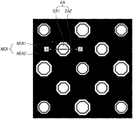
1. An organic light emitting display panel comprising:
a substrate including an active area and a non-active area;
a transistor in the active area of the substrate;
an insulating film disposed over the transistor in the active area of the substrate; and
a sub-pixel electrically connected to the transistor, the sub-pixel including a plurality of light emitting areas comprising a first light emitting area and a second light emitting area where each of the first light emitting area and the second light emitting area has one of a first width or a second width, and a separation area that is non-light emitting is disposed between the first light emitting area and the second light emitting area of the sub-pixel such that the first light emitting area is separated from the second light emitting area by the separation area, the separation area having a third width that is different from the first width and the second width.
|