| CPC H10K 59/122 (2023.02) [C09D 11/30 (2013.01); C09K 11/06 (2013.01); H10K 71/00 (2023.02); H10K 85/141 (2023.02); H10K 59/1201 (2023.02)] | 14 Claims |
|
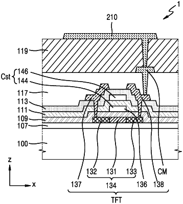
1. A method of manufacturing a display device, the method comprising the steps of:
forming a pixel electrode on a substrate;
forming a bank layer on the pixel electrode, the bank layer having an opening exposing at least part of the pixel electrode; and
forming an intermediate layer on the pixel electrode by discharging ink comprising an organic material onto the pixel electrode,
wherein the organic material has a molecular weight greater than about 500 and less than about 1,000,000 g/mol, and
the organic material in the ink has a concentration and the molecular weight of the organic material satisfy:
y>−3.518*ln(x)+45.59,
wherein y is the concentration of the organic material, and x is the molecular weight of the organic material.
|