| CPC H10K 59/1216 (2023.02) [H10K 59/1201 (2023.02)] | 13 Claims |

|
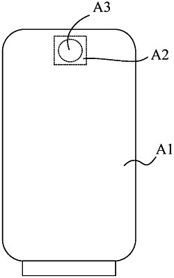
1. A display substrate, comprising a base substrate, a driving circuit layer and a light-emitting unit, wherein the driving circuit layer and the light-emitting unit are located on the base substrate, the light-emitting unit comprises a first electrode and a second electrode that are laminated on each other, and a light-emitting layer located between the first electrode and the second electrode; the display substrate comprises a first display region, a second display region, and an opening region; the second display region is located between the first display region and the opening region; and a pixel density of the first display region is greater than a pixel density of the second display region; and
the display substrate further comprises a compensation capacitor configured for compensating a sub-pixel in the second display region, wherein the compensation capacitor comprises a first plate and a second plate, the first plate is electrically connected to a gate electrode of the sub-pixel in the second display region, and the second plate is electrically connected to the first electrode;
the driving circuit layer comprises a gate layer;
wherein in a direction away from the base substrate, the gate layer of the driving circuit layer comprises a first gate metal layer and a second gate metal layer, one plate of the first plate and the second plate of the compensation capacitor is provided in a same layer and made of a same material as the first gate metal layer, and the other plate of the compensation capacitor is provided in a same layer and made of a same material as the second gate metal layer.
|