| CPC H10K 50/854 (2023.02) [H01L 25/0753 (2013.01); H01L 33/06 (2013.01); H01L 33/14 (2013.01); H01L 33/382 (2013.01); H10K 50/115 (2023.02); H10K 50/15 (2023.02); H10K 50/16 (2023.02); H10K 50/17 (2023.02); H10K 50/818 (2023.02); H10K 50/822 (2023.02); H10K 50/828 (2023.02); H10K 71/00 (2023.02); H10K 71/621 (2023.02); H01L 2933/0016 (2013.01); H10K 2102/103 (2023.02); H10K 2102/3026 (2023.02)] | 6 Claims |
|
1. A fabrication method of a light-emitting diode structure, comprising:
providing a base substrate;
sequentially forming a first electrode layer and a light-emitting layer on the base substrate;
arranging a first mask and a second mask which are stacked with each other on a side of the light-emitting layer facing away from the base substrate, a spacing being set between the first mask and the second mask; and
forming a second electrode layer on the base substrate on which the first electrode layer and the light-emitting layer are formed by adopting the first mask and the second mask,
wherein the first mask includes at least one first opening and a first shielding portion surrounding the at least one first opening, the second mask includes a plurality of second openings and a second shielding portion surrounding the plurality of second openings, and orthogonal projections of the plurality of second openings on the first mask are located within the at least one first opening,
forming the second electrode layer on the base substrate on which the first electrode layer and the light-emitting layer are formed by adopting the first mask and the second mask includes:
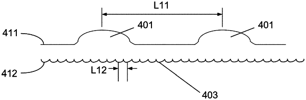
enabling the electrode material to sequentially pass through each second opening of the second mask and the at least one first opening of the first mask so as to form the second electrode layer, a plurality of protrusions being formed on the surface of the second electrode layer away from the base substrate.
|