| CPC H10K 50/824 (2023.02) [H10K 59/122 (2023.02); H10K 71/00 (2023.02); H10K 50/818 (2023.02); H10K 50/828 (2023.02); H10K 59/1201 (2023.02); H10K 2102/103 (2023.02); H10K 2102/3026 (2023.02)] | 18 Claims |
|
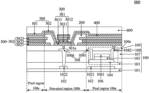
1. A display panel, comprising:
a substrate;
a pixel-defining layer disposed on the substrate; and
a conductive pattern, a light-emitting layer and a cathode layer which are laminated in a direction perpendicular to and away from the substrate,
wherein the pixel-defining layer is configured to define a plurality of pixel regions and a non-pixel region outside the pixel regions on the substrate;
the conductive pattern comprises: an auxiliary electrode layer disposed in the non-pixel region, wherein a groove is formed in a side wall of the auxiliary electrode layer; and
the cathode layer comprises: a first portion disposed in the pixel region and a second portion disposed in the non-pixel region, wherein the second portion of the cathode layer extends into the groove and is in contact with the groove; and
wherein,
the auxiliary electrode layer comprises a metal electrode and a first protective electrode which are laminated in the direction perpendicular to the substrate, and the first protective electrode is disposed at a side away from the substrate of the metal electrode; and in a direction parallel with the substrate, the first protective electrode is extended over the metal electrode to form the groove and the second portion of the cathode layer is in contact with a side wall of the metal electrode; and
the auxiliary electrode layer further comprises a second protective electrode disposed at a side of the metal electrode closer to the substrate; in the direction parallel with the substrate, the second protective electrode is extended over the metal electrode to form the groove, and the second portion of the cathode layer is disposed in the groove and is in contact with the second protective electrode.
|