| CPC H10K 50/00 (2023.02) [G09G 3/006 (2013.01); H01L 21/6835 (2013.01); H01L 24/24 (2013.01); H01L 24/75 (2013.01); H01L 24/82 (2013.01); H01L 24/83 (2013.01); H01L 24/97 (2013.01); H01L 27/156 (2013.01); H10K 59/12 (2023.02); G09G 3/3208 (2013.01); H01L 24/32 (2013.01); H01L 27/1214 (2013.01); H01L 2221/68368 (2013.01); H01L 2221/68381 (2013.01); H01L 2224/2401 (2013.01); H01L 2224/245 (2013.01); H01L 2224/2405 (2013.01); H01L 2224/24011 (2013.01); H01L 2224/24137 (2013.01); H01L 2224/24227 (2013.01); H01L 2224/29005 (2013.01); H01L 2224/29109 (2013.01); H01L 2224/29111 (2013.01); H01L 2224/29113 (2013.01); H01L 2224/29118 (2013.01); H01L 2224/29124 (2013.01); H01L 2224/29139 (2013.01); H01L 2224/29144 (2013.01); H01L 2224/29147 (2013.01); H01L 2224/29155 (2013.01); H01L 2224/32014 (2013.01); H01L 2224/32057 (2013.01); H01L 2224/32237 (2013.01); H01L 2224/32503 (2013.01); H01L 2224/759 (2013.01); H01L 2224/7565 (2013.01); H01L 2224/7598 (2013.01); H01L 2224/75252 (2013.01); H01L 2224/75301 (2013.01); H01L 2224/75725 (2013.01); H01L 2224/82101 (2013.01); H01L 2224/82102 (2013.01); H01L 2224/82104 (2013.01); H01L 2224/83 (2013.01); H01L 2224/83005 (2013.01); H01L 2224/8381 (2013.01); H01L 2224/8383 (2013.01); H01L 2224/83192 (2013.01); H01L 2224/83193 (2013.01); H01L 2224/83203 (2013.01); H01L 2224/83805 (2013.01); H01L 2224/83825 (2013.01); H01L 2224/97 (2013.01); H01L 2924/0781 (2013.01); H01L 2924/12041 (2013.01); H01L 2924/12042 (2013.01); H01L 2924/12044 (2013.01); H10K 59/10 (2023.02)] | 17 Claims |
|
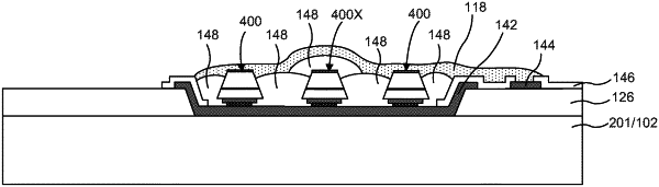
1. A display panel redundancy scheme comprising:
a display substrate;
a first micro light emitting diode (LED) and a second micro LED arranged within a subpixel;
wherein the first micro LED and the second micro LED each comprises a p-n diode, a top conductive contact, and a bottom conductive contact that is bonded to the display substrate;
a passivation material over the second micro LED; and
a top electrode layer over the first micro LED and the second micro LED, wherein the top electrode layer is in electrical contact with the first micro LED and the passivation material physically separates the top electrode layer from the top conductive contact of the second micro LED.
|