| CPC H10K 30/82 (2023.02) [H10K 30/30 (2023.02); H10K 39/32 (2023.02)] | 19 Claims |
|
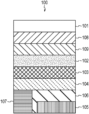
1. A photoelectric conversion element, comprising:
a first electrode;
a work function control layer that contains a hexavalent molybdenum oxide, a pentavalent molybdenum oxide, and a tetravalent molybdenum oxide, wherein
the work function control layer has a larger amount of oxygen than an amount of oxygen satisfying a stoichiometric composition, and
an amount of the hexavalent molybdenum oxide is larger than a total amount of the pentavalent molybdenum oxide and the tetravalent molybdenum oxide;
a photoelectric conversion layer;
an oxide semiconductor layer;
a second electrode, wherein the first electrode, the work function control layer, the photoelectric conversion layer, the oxide semiconductor layer, and the second electrode are in this order;
an insulating layer; and
a third electrode, wherein
the third electrode is apart from the second electrode, and
the third electrode faces the photoelectric conversion layer via the insulating layer.
|
|
11. A photoelectric conversion element, comprising:
a first electrode;
a work function control layer that contains
a hexavalent molybdenum oxide, a pentavalent molybdenum oxide, and a tetravalent molybdenum oxide, and
an oxide containing molybdenum and at least one metal element different from the molybdenum,
wherein the work function control layer has a larger amount of oxygen than an amount of oxygen satisfying a stoichiometric composition;
a photoelectric conversion layer;
an oxide semiconductor layer;
a second electrode, wherein the first electrode, the work function control layer, the photoelectric conversion layer, the oxide semiconductor layer, and the second electrode are in this order;
an insulating layer; and
a third electrode, wherein
the third electrode is apart from the second electrode, and
the third electrode faces the photoelectric conversion layer via the insulating layer.
|