| CPC H10B 63/84 (2023.02) [H10N 70/063 (2023.02); H10N 70/231 (2023.02); H10N 70/826 (2023.02); H10N 70/841 (2023.02); H10N 70/8616 (2023.02)] | 20 Claims |
|
1. A method comprising:
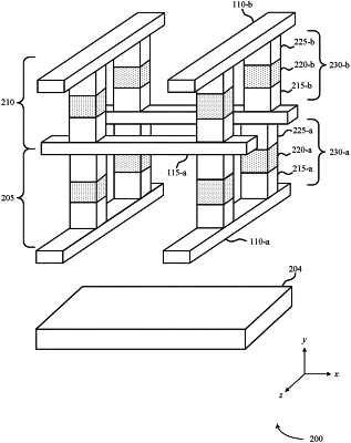
depositing a first resistive material on a plurality of memory stacks, each of the memory stacks including a layered assembly of electrode materials and a memory material;
depositing, on the plurality of memory stacks over the first resistive material, a first conductive material;
removing an area of the plurality of memory stacks to form a gap in the first resistive material, the first conductive material, and one or more memory stacks of the plurality of memory stacks;
depositing a conductive material to form a conductive via in the gap;
depositing, over the first conductive material and the conductive via, a second resistive material; and
depositing, on the plurality of memory stacks over the second resistive material and on the conductive via over the second resistive material, a second conductive material.
|