| CPC H10B 43/27 (2023.02) [H10B 41/27 (2023.02); H10B 41/35 (2023.02); H10B 41/41 (2023.02); H10B 43/35 (2023.02); H10B 43/40 (2023.02)] | 20 Claims |
|
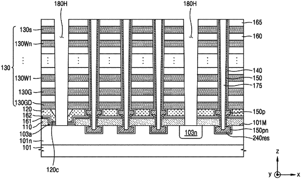
1. A method of fabricating a vertical semiconductor device, the method comprising:
forming a lower sacrificial layer pattern on a substrate;
forming a support layer on the lower sacrificial layer pattern;
alternately stacking a sacrificial layer and an insulating layer on the support layer;
forming a channel hole penetrating the sacrificial layer, the insulating layer, the support layer, and the lower sacrificial layer pattern;
partially removing an exposed sidewall of the support layer in the channel hole;
forming an information storage material layer and a channel pattern in the channel hole so that the information storage material layer and the channel pattern fill a space formed by partially removing the exposed sidewall of the support layer in the channel hole;
replacing the lower sacrificial layer pattern with a common source semiconductor layer; and
replacing the sacrificial layer with gates.
|