| CPC H05K 5/0069 (2013.01) [H05K 1/111 (2013.01); H05K 1/148 (2013.01); H05K 5/0018 (2022.08); H05K 2201/09418 (2013.01)] | 22 Claims |
|
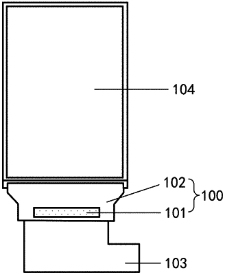
1. A chip packaging structure, comprising at least one chip packaging unit, the chip packaging unit comprising:
a flexible substrate, the flexible substrate comprising a first flexible substrate body, a plurality of first traces arranged on the first flexible substrate body, and a plurality of input pads and a plurality of output pads arranged on the first flexible substrate body, the plurality of input pads and the plurality of output pads being connected in one-to-one correspondence through the first traces; and
a rigid substrate, the rigid substrate comprising a rigid substrate body and a chip arranged on the rigid substrate body;
wherein the rigid substrate is bonded to a drive printed circuit board of a display device;
a side of the flexible substrate is bonded to the rigid substrate, and another side of the flexible substrate is bonded to a display panel of the display device; and the plurality of input pads are electrically connected to the chip, and the plurality of output pads are configured to transmit signals to the display panel.
|