| CPC H04W 4/90 (2018.02) [G08B 6/00 (2013.01); H04M 1/0202 (2013.01); G06F 3/041 (2013.01); G06F 3/044 (2013.01); G09G 2310/0267 (2013.01); H04M 2250/12 (2013.01)] | 14 Claims |
|
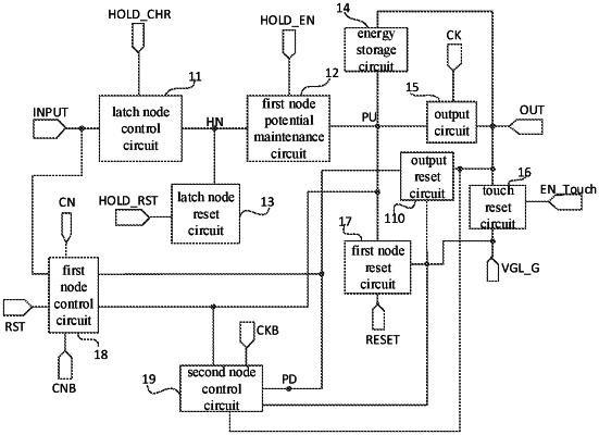
1. A gate driving unit, comprising an input terminal, a latch node control circuit, a first node potential maintenance circuit, and a latch node reset circuit, wherein
the latch node control circuit is respectively connected to a latch node, the input terminal, and a latch charging terminal, and is configured to control a voltage of the latch node through a charging voltage inputted by the latch charging terminal under the control of an input signal provided by the input terminal,
the first node potential maintenance circuit is respectively connected to the latch node, a first node, and a latch enable terminal, and is configured to control the connection between the first node and the latch enable terminal under the control of a voltage of the latch node, to maintain a potential of the first node; and
the latch node reset circuit is respectively connected to a latch node reset terminal and the latch node, and is configured to control to reset the potential of the latch node under the control of the latch node reset signal inputted by the latch node reset terminal,
wherein the gate driving unit further comprises a gate driving signal output terminal, an energy storage circuit, an output circuit, a touch reset circuit, and a first node reset circuit,
a first terminal of the energy storage circuit is connected to the first node, a second terminal of the energy storage circuit is connected to the gate driving signal output terminal, and the energy storage circuit is configured to control the potential of the first node;
the output circuit is respectively connected to the first node, the gate driving signal output terminal and a first clock signal terminal, and is configured to control the connection between the gate driving signal output terminal and the first clock signal terminal under the control of the voltage of the first node;
the touch reset circuit is respectively connected to a touch reset terminal, the gate driving signal output terminal and a reset voltage terminal, and is configured to control the connection between the gate driving signal output terminal and the reset voltage terminal under the control of the touch reset signal inputted by the touch reset terminal; and
the first node reset circuit is respectively connected to a blank area reset terminal, the first node and the reset voltage terminal, and is configured to control the connection between the first node and the reset voltage terminal under the control of a blank area reset signal inputted by the blank area reset terminal.
|