US 11,778,343 B2
Methods and circuitry for improving global shutter efficiency in backside illuminated high dynamic range image sensor pixels
Dajiang Yang, San Jose, CA (US); Sergey Velichko, Boise, ID (US); Bartosz Piotr Banachowicz, San Jose, CA (US); Tomas Geurts, Haasrode (BE); and Muhammad Maksudur Rahman, Santa Clara, CA (US)
Assigned to SEMICONDUCTOR COMPONENTS INDUSTRIES, LLC, Scottsdale, AZ (US)
Filed by SEMICONDUCTOR COMPONENTS INDUSTRIES, LLC, Phoenix, AZ (US)
Filed on Nov. 30, 2021, as Appl. No. 17/456,982.
Application 17/456,982 is a continuation of application No. 16/661,009, filed on Oct. 23, 2019, granted, now 11,218,653.
Claims priority of provisional application 62/871,899, filed on Jul. 9, 2019.
Prior Publication US 2022/0086375 A1, Mar. 17, 2022
This patent is subject to a terminal disclaimer.
Int. Cl. H04N 25/58 (2023.01); H04N 25/63 (2023.01); H01L 27/146 (2006.01)
CPC H04N 25/58 (2023.01) [H01L 27/1464 (2013.01); H01L 27/14627 (2013.01); H01L 27/14656 (2013.01); H04N 25/63 (2023.01)] 19 Claims
OG exemplary drawing
 
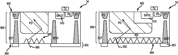
1. An image sensor comprising:
a photodiode in a front side of a substrate and configured to accumulate charge generated by scenery light;
a first storage node configured to store the accumulated charge from the photodiode;
a second storage node configured to store charge generated by parasitic light; and
optical diffracting structures in a back side of the substrate.