| CPC H03K 17/6872 (2013.01) [H02M 1/08 (2013.01); H02P 7/04 (2016.02)] | 8 Claims |
|
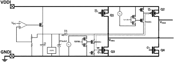
1. A circuit, comprising:
a first PMOS high-side transistor device;
a first NMOS low-side transistor device; and
turn-on circuitry configured to turn on the first PMOS high-side transistor device while simultaneously turning on the first NMOS low-side transistor device, by routing charge stored in a gate of the first PMOS high-side transistor device to a gate of the first NMOS low-side transistor device, to charge the gate of the first NMOS low-side transistor device.
|