| CPC H03K 17/6871 (2013.01) [G06N 10/20 (2022.01); H03D 7/1425 (2013.01); H03K 5/02 (2013.01); H03K 5/1252 (2013.01)] | 25 Claims |
|
1. A device, comprising:
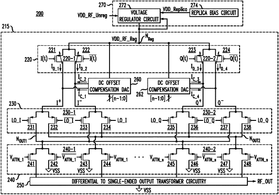
a voltage-mode filter circuit which is configured to generate a voltage signal on an output terminal thereof;
a current-mode output circuit comprising an input transistor which comprises a gate terminal coupled to the output terminal of the voltage-mode filter circuit, and a source terminal coupled to a regulated node; and
a regulation circuit configured to adjust a voltage level on the regulated node to maintain a constant gate-source bias voltage for the input transistor to generate a current for biasing the current-mode output circuit.
|