| CPC H03K 17/04123 (2013.01) | 19 Claims |
|
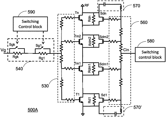
1. A radio frequency (RF) field effect transistor (FET) switch stack comprising:
FET transistors arranged in a stacked configuration;
one or more first drain-source resistors, each first drain-source resistor coupled across drain-source terminals of a corresponding FET transistor of the FET transistors;
one or more drain-source bypass switches, each drain-source bypass switch coupled across corresponding one or more first drain-source resistors; and
a switching control block configured to control the drain-source bypass switches, the switching control block comprising one or more FET control switches configured to be in a control switch OFF state when the FET transistors are in a stack OFF state or a stack ON state and to be in a control switch ON state when the FET transistors are transitioning from the stack ON state to the stack OFF state.
|