| CPC H01Q 1/38 (2013.01) [H01L 21/4853 (2013.01); H01L 21/4857 (2013.01); H01L 21/565 (2013.01); H01L 21/568 (2013.01); H01L 23/3121 (2013.01); H01L 23/5383 (2013.01); H01L 23/5386 (2013.01); H01L 23/5389 (2013.01); H01L 23/552 (2013.01); H01L 23/66 (2013.01); H01L 24/19 (2013.01); H01L 24/20 (2013.01); H05K 1/115 (2013.01); H01L 2223/6677 (2013.01); H01L 2224/214 (2013.01); H01L 2924/19105 (2013.01); H01L 2924/3025 (2013.01); H01Q 9/16 (2013.01); H05K 2201/10015 (2013.01); H05K 2201/10098 (2013.01); H05K 2201/10522 (2013.01); H05K 2201/10545 (2013.01)] | 16 Claims |
|
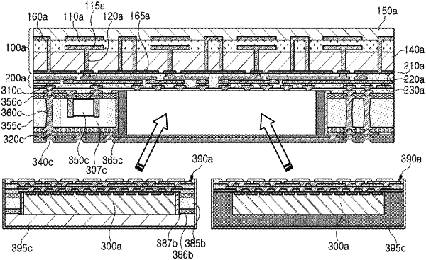
1. An antenna module comprising:
a first connection member having a first surface and a second surface, opposite to the first surface, and including a first wiring layer and a first insulating layer;
an antenna package disposed on the first surface of the first connection member, and including a plurality of antenna members configured to transmit and/or receive a first signal and a plurality of feed vias electrically connecting a corresponding one of the plurality of antenna members to a corresponding wire of the first wiring layer;
an integrated circuit (IC) disposed on the second surface of the first connection member and having an active surface on which a connection pad is disposed, the connection pad being electrically connected to the first wiring layer;
a second connection member disposed between the first connection member and the IC, and including a second wiring layer electrically connecting the first wiring layer to the connection pad of the IC; and
one or more first core vias disposed on the second surface of the first connection member and electrically connected to the first wiring layer so that a second signal different from the first signal passes therethrough,
wherein the second connection member has a third surface facing the second surface, a fourth surface opposite to the third surface and in direct contact with the active surface, and a side surface extending between the third surface and the fourth surface,
wherein the side surface of the second connection member is surrounded by the one or more first core vias.
|