| CPC H01L 29/7869 (2013.01) [H01L 21/02532 (2013.01); H01L 21/02565 (2013.01); H01L 21/385 (2013.01); H01L 21/44 (2013.01); H01L 27/1225 (2013.01); H01L 27/1259 (2013.01); H01L 29/267 (2013.01); H01L 29/66969 (2013.01); H01L 29/78606 (2013.01); H01L 29/78618 (2013.01)] | 16 Claims |
|
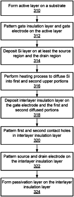
1. A method of manufacturing a thin film transistor, comprising:
forming an active layer of oxide semiconductor on a substrate, the active layer including a channel region, a source region at one side of the channel region, and a drain region at the other side of the channel region;
forming a gate insulating material on the substrate in which the active layer is formed;
forming a gate metallic layer on the substrate in which the gate insulating material is formed;
forming a gate insulating layer and a gate electrode overlapping with the channel region of the active layer by patterning the gate metallic layer and the gate insulating material, wherein forming the gate insulating layer includes a dry etching process, wherein oxygen contained in the source region and the drain region is released by an etchant gas used in the dry etching process, such that the source region and the drain region of the active layer become conductive;
forming an oxidation preventing film at an upper portion of each of the source region and the drain region by adding Si into the upper portion of each of the source region and the drain region; and
forming an interlayer insulating layer on the gate electrode and the active layer including the oxidation preventing film.
|