| CPC H01L 29/7813 (2013.01) [H01L 29/0696 (2013.01); H01L 29/404 (2013.01); H01L 29/45 (2013.01); H01L 29/495 (2013.01); H01L 29/4916 (2013.01); H01L 29/66734 (2013.01)] | 17 Claims |
|
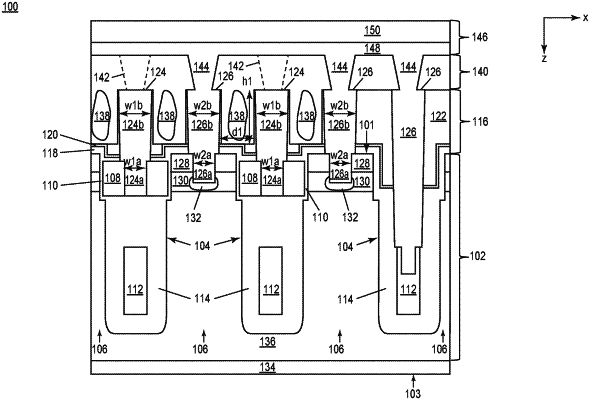
1. A semiconductor device, comprising:
a Si substrate having a first main surface;
a plurality of gate trenches extending from the first main surface into the Si substrate;
a semiconductor mesa between adjacent gate trenches;
a first interlayer dielectric on the first main surface;
a plurality of first metal contacts extending through the first interlayer dielectric and contacting gate electrodes disposed in the gate trenches;
a plurality of second metal contacts extending through the first interlayer dielectric and contacting the semiconductor mesas; and
an air gap or a dielectric material having a lower dielectric constant than the first interlayer dielectric between adjacent first and second metal contacts.
|